Research Fields and Projects
Optoelectronics
Our vision for the future of optoelectronics
Driving innovation in optoelectronics
We, the optoelectronics team at ILO – HSEL, are passionate about pushing the boundaries of technology and developing breakthrough solutions that will shape the world of tomorrow.
Ongoing and completed projects
Non-Linear response of single turn plasmonic nano helix antenna (2025)
The intrinsic chrality of helices offers sensitivity to the handedness of circular polarized light. The non-linear response has potential to offer even more insight and open new pathways for plasmonic based sensing of chiral properties or vice versa – generation of circular polarized light.
This is investigated by creation of ultrashort IR laser pulses with either LHC or RHC polarization and directing it onto a single gold nono helix. The non-linear response in the VIS is then observed by a spectrometer.
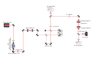
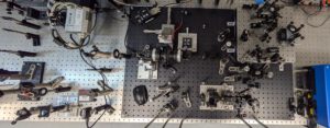
The project is currently being prepeared, and we expect notable results in the near future.
– Magnus Hudalla
Measurement for fluorescent behavior of quantum dots (2025)
Making an experiment to analyse the fluorescent behaviour of quantum dots and afterwards exploring the possibility of implementing quantum dots as single photon emitters.
An optical setup using a white lase by the fianum company to excite quantum dots.
— Finn Hahn
Fan gratings for plasmonic multiplexing (2025)
The idea behind this project is to use a fan-shaped grating to couple different wavelengths depending on the position of a light spot on the grating. In combination with a second grating for outcoupling, this setup forms a multiplexer/demultiplexer system for light.
A spectroscopy setup is used to analyze the spectrum of the outcoupled light in terms of wavelength and intensity. This analysis is performed for different grating parameters and shapes of the outcoupling grating.
– Max Schwabe
Fiber Ball Lens Systems (2025)
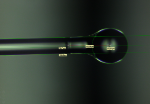
I am currently working on fiber ball lens systems (FBLS) as a part of my bachelor’s thesis. These FBLS could in theory be used to bypass bulky optical setups that are used to focus laser light down to a small spot size (around 10 microns in diameter).
The difficult and interesting part of these FBLS is the manufacturing process. The margins for the desired optical properties are in the range of microns, which makes producing them very tricky. In my work, I want to figure out if there is a feasible way to produce these FBLS with the equipment available.

– Martin Backer
Fabrication and optical characterization of plasmonic Bulls Eye cavities (2024-2025)
The idea is to efficiently capture and guide far-field propagating light into a sub-wavelength region in the middle of a circular-shaped bulls-eye plasmonic cavity. When placing atomically-thin transistion-metal dichalcogenide (TMDC) films on top of these cavities with dimensions of a few tens of micrometers, one can enhance the generation single photon events from these TMDC films significantly. In addition to that a careful design of the metallic bulls eye cavity can be used to steer the emission of light into a narrow angle perpendicular to the TMDC surface.
The electric field distribution from these plasmonic bulls eye cavities are first simulated using computer-based finite-difference time-domain simulations. Based on these findings, bulls eye cavities with diameters of up to 10 microemters are fabricated using a Gallium-ion focused ion beam approach. The fabricated Bulls-eye cavities are afterwards spectrally characterized in a home-built microscope setup.
– Martin Silies
Characterization of Bulls Eye cavities for use in 2D semiconductor (2024-2025)
Custom design of BE cavities to accommodate their usecase and match certain materials used in single photon sources.
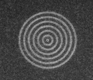

– Simon Koenen
Bachelor or Master thesis
Are you interested in a Bachelor or Master thesis? We certainly can find an exciting topic for you! Please feel free to reach out to Martin Silies.
