
Research Fields and Projects
Optoelectronics
The Plasmonic Transistor – Prof. Dr. rer.nat. Martin Silies
Introduction
In this project we are interested in the interaction of metallic nanostructures with light, e.g. with ultrashort laser pulses. These nanostructures can play a crucial role when focusing electromagnetic waved below the diffraction limit of light. As a result nanometer-sized areas can be generated, in which the electric field strength is order of magnitude larger than in the surrounding region. In principal, the electric field strength is inversely proportional to the antenna distance. This field of enormous strength now allows investigating the interaction of light with few or even singling atoms or quantum emitters.
Fabrication and imaging of the antenna structures
These nanostructures are fabricated by milling them from a very thin, few-nanometer thick gold film using ion beam lithography. Our group is able to fabricate nanostructures using both Helium-ion based and Gallium-ion based ion beam milling. Therefore, very recently we have installed the Orion NanoFab in our laboratories, a Helium-ion based lithography system. In Fig.1, an image of the Orion NanoFab is shown on the left together with a prototypical plasmonic nanostructure that has been fabricated using the Orion (middle image). The Orion NanoFab is not only capable of fabricating nanostructures with nanometer precision but can also image both metallic, i.e., conductive and biological, i.e. nonconductive samples with high magnification.
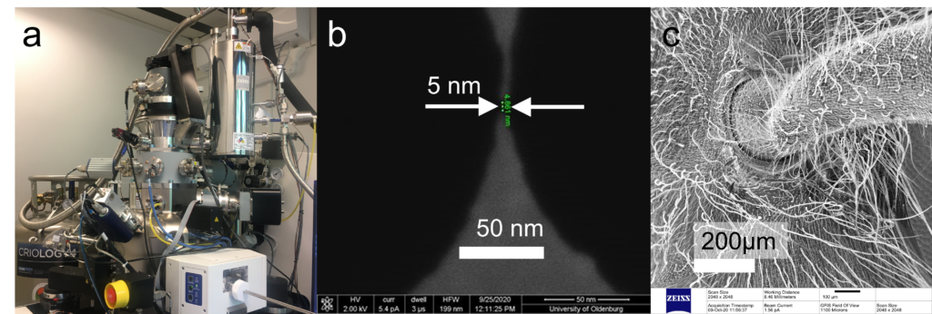
Figure 1: (a) Helium-ion based lithography system Orion NanoFab. (b) Metallic nanostructure fabricated using the Orion. Two micrometer-sized holes are drilled into a 10nm thick-free-standing film. The residual bridge between the two holes was determined to be only 5nm thick. (c) Prototypical example of a wasp antenna.
By using helium ions for the lithography process instead of gallium using the Zeiss Nanofab, sub-10 nm feature sizes in metallic films on a fused silica are now producible. In Fig. 2, these new, highly precise plasmonic antennas using Helium-Ion Lithography are compared to standard gallium-ion beam-produced antennas.
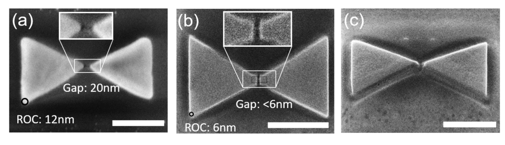
Fig.2 Figure 1: (a) SEM image of an gold bowtie antenna produced using Ga-ion lithography. Herewith, antenna distances of approximately 20 nm can be achieved (b): Helium-Ion microscopy image of an antenna structure with a gap of less than 6 nm using Helium ion lithography In (c), a tited view of this structure is shown.
Nonlinear microscopy with ultrashort laser pulses
We now investigate the interaction by using a spectrally-resolved, nonlinear microscopy (Fig.3). Few-cycle, ultrashort laser pulses from a Ti:Sapphire laser oscillator are focused to their diffraction limit by using an all-reflective Cassegrain objective. The sample is mounted on a piezo stage and can be moved perpendicular to the beam with nm precision. We now detect the third harmonic (TH) of the incident laser light in a spectrometer attached to a liquid-nitrogen cooled CCD camera. The intensity of the TH is herein taken as a measure for the electric field strength within the two components of the nanoantenna.
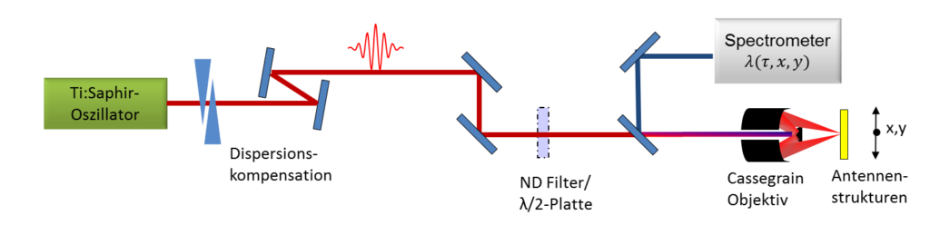
Figure 3: Ultrashort, few-cycle laser pulses from a Ti:Sapphire oscillator are focused to their diffraction limit onto the antenna using an all-reflective Cassegrain objective. The third harmonic is collected in back reflection geometry and analyzed in a spectrometer. The TH here gives a measure for the strength of the electric field within the antenna structure.
Our measurement show that for the antennas produced using helium ion lithography the intensity of the TH increased by a factor of three when compared to the antennas produced using standard Ga-FIB (see Fig. 3(a)). This seems to be especially remarkable, since the emission is originating from an even small volume from the gap region.
FDTD simulations
We simulated the interaction of the light with the nanostructure using a finite element method. These simulations confirm our measurements about the increased confinement of the electric field for the smaller gap structures. In Fig. 4 and, the two-dimensional distribution of the electric field within the nanostructure is shown both for the 20 nm gap antenna produced using Ga-FIB (b) and for the 6 nm antenna produced using helium ions (c). The increase of the field enhancement for the latter structure is clearly visible.
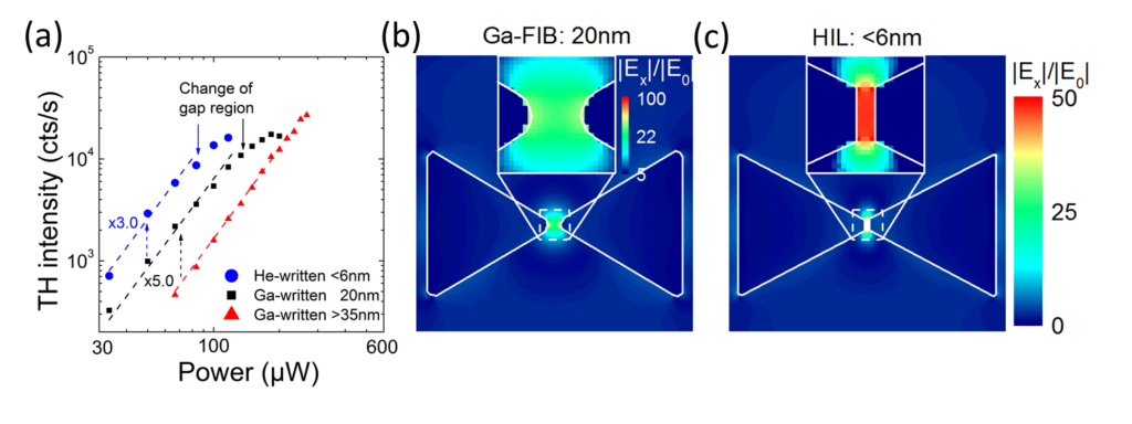
Figure 4(a): Intensity of the third Harmonic from single, He-ion and Ga-ion produced antennas as a function of the excitation power. The TH intensity is increased by a factor of three when using He-ions instead of Ga ions for the fabrication process. (b) and (c): The increase of field enhancement is confirmed within our FEM simulations, in which we calculated the two-dimensional distribution of the electric field within the nanoantennas. The field within the helium-ion produced antennas is enhanced significantly, especially visible in the inset on a logarithmic scale.
These results show the potential of helium-ion based lithography for the production of plasmonic antennas. We are now able to fabricate plasmonic antennas with an unrevealed spatial precision. Plasmonic structures with tailored optical and electronic properties are now within reach. We therefore hope to push the investigation of light-matter interaction to a new limit.